

High-Quality PCB Assembly After Fabrication
The assembly process is a critical part of custom pcb fabrication production. It involves precise component placement and soldering to ensure strong connections. It’s also a highly controlled and audited process, ensuring the product meets industry standards and client expectations.
One way to ensure high-quality assembly is to work with a single expert for the entire process, from design and ordering to fabrication and assembly. This helps to keep communication and project management consistent, making it easier to address any issues that arise along the way. It also gives the assembler a better understanding of your project, and it allows them to create an assembly plan that best suits your needs.
PCB fabrication starts with the printing and etching stage, where engineers remove the unwanted copper from the board to create the circuit pattern. This is a delicate process that requires careful attention to detail, as small mistakes can have a big impact on the overall quality of the finished product.
The next step is drilling and plating, where holes are drilled into the boards to mount components and create vias (holes for additional layers in multi-layer PCBs). This is another critical step, as erroneous holes can lead to short circuits or traces that don’t function properly.
After drilling and plating, the PCB is ready for assembly. This can be done either through Surface Mount Technology (SMT), where the components are placed on the top side of the board and soldered, or through Through Hole Technology (THT), where they’re inserted through holes drilled in the PCB and soldered on the back side.
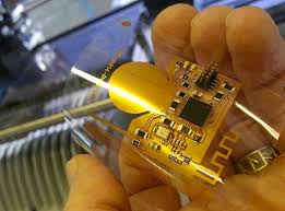
How to Ensure High-Quality PCB Assembly After Fabrication
Before the assembly begins, most PCB fabricators will check the CAD file for any issues that could hinder the production process. This is called a Design for Manufacturability (DFM) check and can help the designer catch problems before they become costly errors in the assembly process.
Another key element of a successful PCB assembly is the use of a high-quality SMT stencil. The stencil is the window through which the solder paste is applied to the board, and it must be clean and clear of any contaminants to ensure the best possible soldering results.
During the assembly process, the assembler will need to carefully inspect each piece of the circuit board to make sure it meets all relevant standards and requirements. This includes visual inspections, automated optical inspection (AOI), and X-ray inspection for more complex PCBs that require greater depth of field.
Another common problem encountered during assembly is erroneous component placement. This can be caused by incorrect footprints, missing polarity indicators on the silkscreen, or inadequate spacing between components. For example, if two components share a pad, it’s important that they’re commensurate in size so the pick and place machine can distinguish them. Otherwise, the result can be “component tombstoning,” where a solder joint isn’t properly formed. For this reason, it’s important to follow guidelines for part-to-component spacing during the design phase.


